| 
Laboratory
Project 3 - Frequency Modulation & Detection
Objectives
This project has 4 parts:
* In Part 1, you will investigate the performance of the slope
detector.
* In Part 2, you will generate FM bandpass signals using the ICL8038
Precision Waveform Generator/Voltage Controlled Oscillator.
* In Part 3, you will use the LM565 Phase-locked-loop for demodulating
FM signals. In all parts, you will test the system with single-tone
FM (with and without added Gaussian noise) and multi-tone FM signals
(without added noise).
* In Part 4, you will use FM Tx and Rx modules to transmit and
receive signals at the proper FM radio frequencies.
Equipment and Software
* HP 33120A Function Generator/Arbitrary Waveform Generator
* HP 8648A RF Signal Generator. Click
here for operation manual
* HP/Agilent Infiniium Oscilloscope
* 1N4148/914 Fast Switching Diode
* ICL8038 Precision Waveform Generator/Voltage Controlled Oscillator.
Download data-sheet here
* LM565 Phase-locked-loop. Download data-sheet
here
* Modular Backplane
* Slope Detector Module
* FM Tx Module. Click here for schematic
and PCB layout
* FM Rx Module. Click here for schematic
and PCB layout
* Assorted Resistors and Capacitors (based on design)
* PC speakers
* Audio Player/PC
* CD or current media format with your favorite legally
acquired music!
* MATLAB (with Instrument Control Toolbox)
* MATLAB Connectivity Functions: >>writefunc(.),
>>scopedat(.)
Click
here for instrument connectivity guide and Matlab function downloads
Instrument Connectivity
In this lab you will be required to send or gather data to/from
various instruments at the station. To do this, you will need an
active connection with the instruments by opening and refreshing
the instruments in Agilent IO Libraries. Click Start>All Programs>Agilent
IO Libraries Suite>Agilent Connection Expert. When the software
is open, click the refresh button until the instrument icons are
green. Obvioulsy the instruments will need to be powered on and
past initialization before they are seen by Connection Expert.
You will also need the board index (the 'number' of the interface
card), and the GPIB address of the instrument. To find the board
index, open the tmtool link under Matlab>Start>Toolboxes>Instrument
Control>Test and Measurement Tool (tmtool) OR type >>tmtool
in the Matlab command window. Expand the Hardware and then the GPIB
tab on the lefthand pane. The board index should be either 7 or
8. You will see that boards that have instruments connected to them
will be expandable. The GPIB addresses are consistent across all
instruments in the Mixed Signals Laboratory:
Oscilloscope: 7
HP8648A: 9
HP33120A (Upper): 10
HP33120A (Lower): 11
HP34970A: 12
Keithley 2000/2100: 16
HP/Agilent E3631A: 5
->
Please read the full connectivity guide for further details
Part 1
Project Requirements
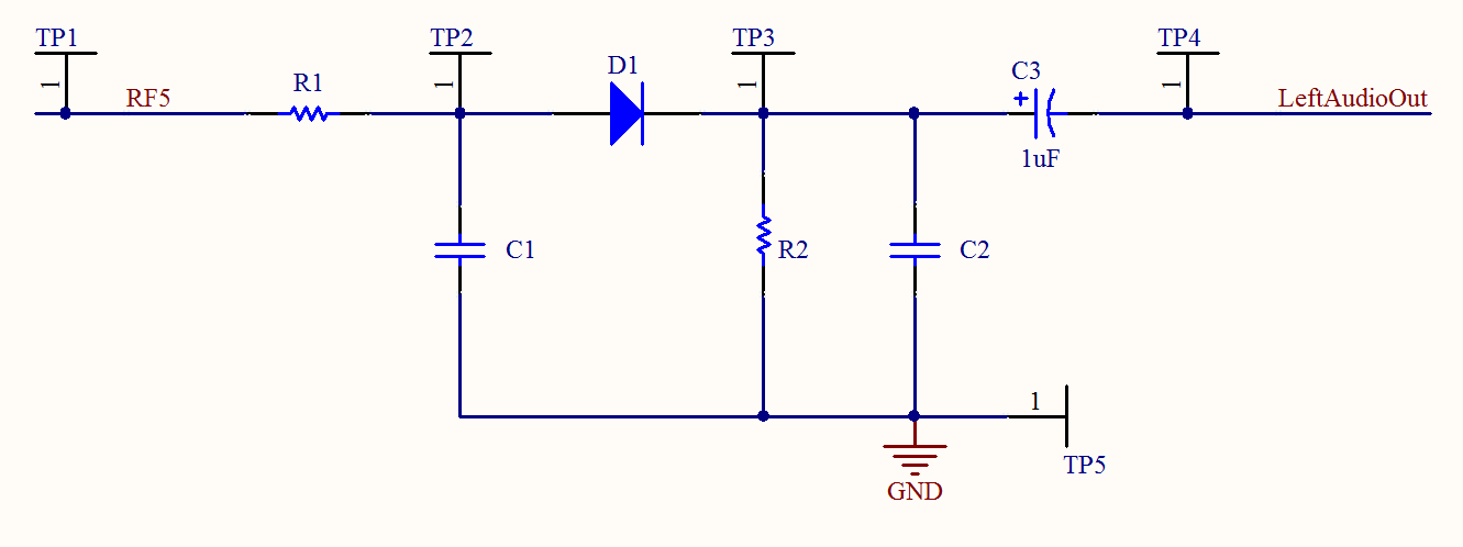
* Design the slope detector circuit shown in Figure 1. The slope
detector is nothing but a frequency-to-voltage converter followed
by an AM envelope detector.The design equation for the frequency-to-amplitude
converter is given by:

fco is chosen to be at the carrier frequency of the
FM signal. The design equation for the envelope detector circuit
is similar and was provided in Lab Project 2. As before, C3 is
a coupling capacitor, chosen such that C3 >> C2 . As part
of your initial design parameters, you can choose an FM carrier
frequency of 30kHz and a maximum modulating frequency of 15kHz
to design your circuit.
Figure 1: Slope detector circuit. click to enlarge
* Using the HP Arb. Function Generator, generate an FM wave
with carrier frequency of 30kHz and modulation frequency 1kHz
(single tone).
- Vary the frequency deviation and observe the input and output
waveforms.
- Vary the modulating frequency and observe the input and output
waveforms.
- Determine the range of performance of the slope detector,
in terms of modulation frequency and modulation index.
- Digitally capture samples of the input and output waveforms
in this range
- Perform a spectral analysis of these input and output waveforms.
- Listen to the output signal using the PC speakers. Compare
with the pure tone of the same frequency.
* Repeat the experiment by digitally synthesizing FM signals
with varying SNR.
* At each stage, note your obervations and conclusions.
Part 2
The objective in Part 2 is to generate single- and multi-tone
FM signals using a voltage controlled oscillator and observe the
waveforms in the time and spectral domains.
* Implement the Frequency Modulator circuit shown in the data
sheet (reproduced in Figure 2 below). The output of the VCO
when no modulation is applied (i.e. the carrier frequency) is
given by f = 0.33/RC, where R = RA = RB =
RL. Design the circuit for a carrier frequency of 30
kHz. Test the system response by feeding a 1Hz audio-frequency
tone to the FM sweep input pin. Observe the waveforms on the
oscilloscope.
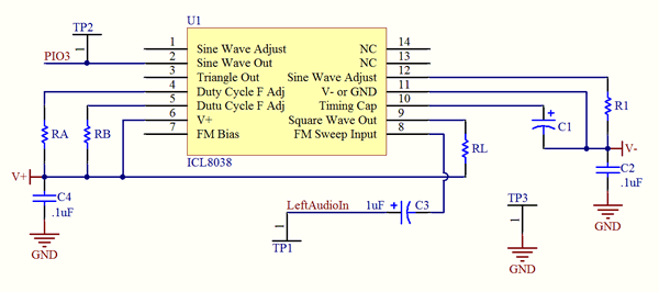
Figure 2: Frequency modulation application circuit from ICL8038
data-sheet. click to enlarge
* Experiment with varying the modulating signal frequency
and amplitude. Oberve the input and output waveforms.
* Determine the range of modulation indices and modulating
frequencies at which this circuit will operate. Digitally capture
a few input/output waveforms in this range and perform spectral
analysis. Confirm your obervations with theoretical predictions.
* Experiment with feeding in multi-tone modulating signals
at the modulating signal input of this circuit.
* Use the slope detector circuit you have designed in Part
1 to recover the baseband signal (for both single- and multi-tone).
Observe and listen.
Part 3
The objective in Part 3 is to demodulate an FM signal using a
voltage controlled oscillator and observe the waveforms in the
time and spectral domains.
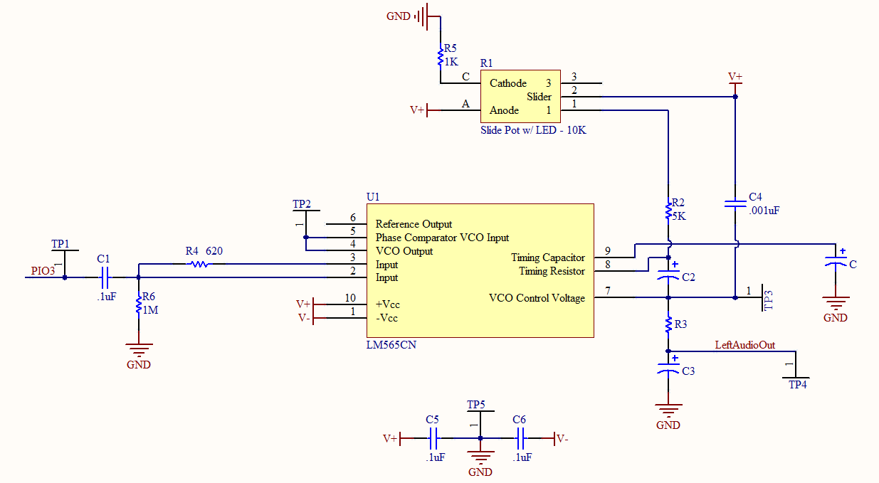
* Design the test circuit shown in Figure 3. Choose the free-running
frequency of the Phase Locked Loop (PLL) equal to the carrier
frequency of the FM signal. The design equation is f0
= 0.3/RC, where R = R1 + R2. C2 is coupling for the timing resistor.
The value can be selected as 0.001uF.
R3 and C3 form a simple LPF for the output (which we hope is
your recovered message signal).
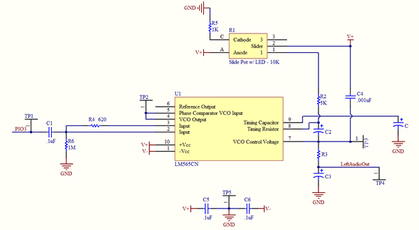
Figure 3: FM demodulator circuit using the LM565 PLL. click
to enlarge
* Use a 9V rail.
* Test the circuit by feeding in an FM signal from the arbitrary
function generator, observe (waveform and spectrum) and listen
to the audio output. Vary the input signal amplitude, the modulating
signal frequency and the modulation index. Experiment with the
capture range and lock range of the PLL.
* Test the product detector circuit by feeding digitally synthesized
FM signals with varying SNR. When does the demodulator fail
to detect the message signal?
* Link the modulator-demodulator circuits and observe signal
progression from input to output. You will need to use an op-amp
buffer circuit between the two circuits so that the demodulator
does not overload the VCO output.
Part 4
The objective in Part 4 is similar to Part 3: characterizing
the performance of the modulator and demodulator. We will use
FM Tx (transmitter - modulator) and Rx (receiver - demodulator)
modules that can operate at the proper MHz ranges that typical
FM radio bands use.
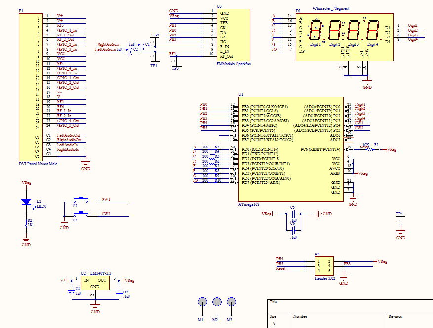
* Test the Rx module shown in Figure 4 by feeding in an FM
signal from the 8648A RF signal generator. The FM carrier should
be selected in the FM radio band (87.5 to 108 MHz). The 8648A
signal generator (just the like the 33120A) can generate FM
signals from either internal or external modulation sources.
Click here for the HP 8648A operation
manual.
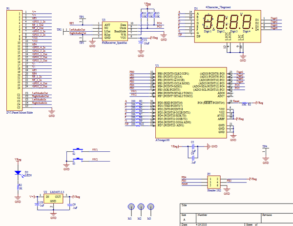
Figure 4: FM Rx module schematic, click to enlarge, Click
here for schematic and PCB layout
* When does the FM Rx module fail to detect the message signal?
* Observe (waveform and spectrum) and listen to the audio output.
* Install the Tx module shown in Figure 5 and view the modulated
spectrum.
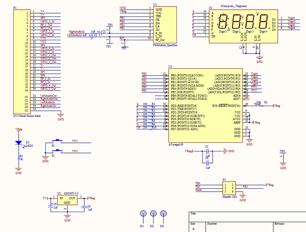
Figure 5: FM Tx module schematic, click to enlarge, Click
here for schematic and PCB layout
* Determine the range of modulation indices and modulating
frequencies at which this circuit will operate. Digitally capture
input/output waveforms in this range and perform spectral analysis.
Confirm your obervations with theoretical predictions.
* Link the modulator-demodulator circuits and observe signal
progression from input to output.
Required Reading
* Sections 4.13, 4.14 and 5.6 of textbook.
* User's Guides for HP/Agilent 33120A Function Generator/Arbitrary
Waveform Generator, User Manual for HP 8648A RF Signal Generator,
Agilent Infiniium Series Oscilloscopes
Click
here for required lab project report format.
Click
here for suggestions for a good lab report.
References:
* HP 33120A Function Generator/Arbitrary Waveform Generator
User's Guide
* Appendix B (p. 650) in textbook
* Zsolt Papay, Technical University of Budapest (TUB),"Experiments
in Gaussian White-noise Generation," HP Test and Measurements
Educator's Corner, http://www.home.agilent.com/upload/cmc_upload/All/Exp65.pdf
* Chapter 4, 5 in the texbook.
* MATLAB Demos: http://users.rowan.edu/~shreek/spring10/ecomms/demos.html
|